
Samsung Discovered a Material for Semiconductors
South Korea-based technology giant Samsung announced that it has discovered a new material called amorphous boron nitride (a-BN). Samsung Advanced…

South Korea-based technology giant Samsung announced that it has discovered a new material called amorphous boron nitride (a-BN). Samsung Advanced…
South Korea-based technology giant Samsung, amorphous boron nitride He announced that he had discovered a new material called (a-BN). Researchers at Samsung Advanced Institute of Technology (SAIT) worked with Ulsan National Institute of Science and Technology (UNIST) and University of Cambridge to realize this discovery.
The findings obtained from this joint study were published in the journal Nature. Researchers, the material will accelerate the development of new generation semiconductors he thinks.
The development of semiconductors will accelerate
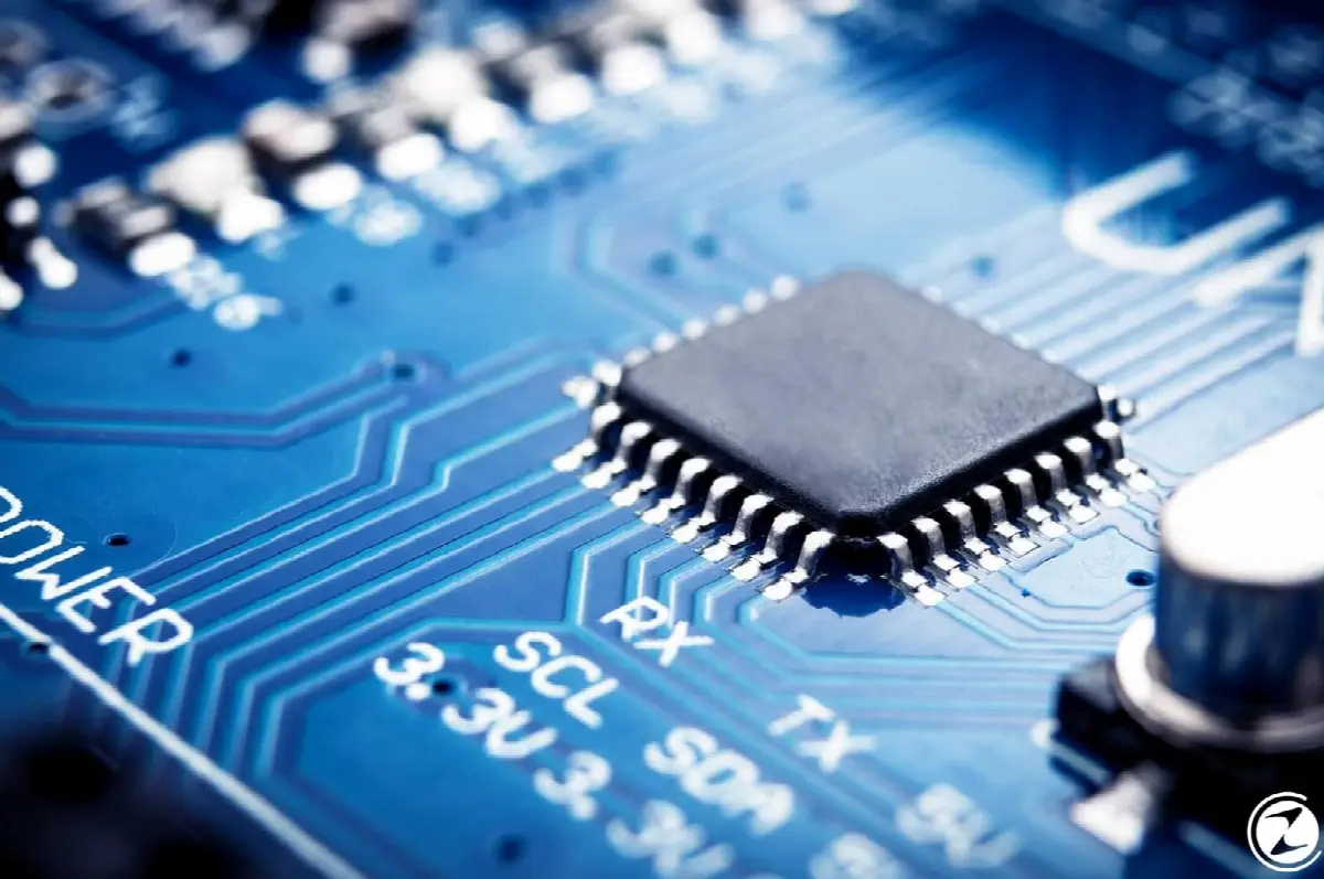
The technology giant stated that the newly discovered amorphous boron nitride contains boron and nitrogen atoms with an irregular molecular structure. SamsungHe said that the new material was obtained from white graphene, but its different molecular structure makes amorphous boron nitride unique.
Korean company, electrical interference He stated that they expect a-BN to be used in DRAM and NAND solutions, thanks to its ability to minimize and grow at a fine scale at a relatively low temperature of 400 degrees. SAIT graphene project manager Hyeon-Jin Shin said:
"To improve the compatibility of graphene with silicon-based semiconductor processes, thin-scale graphene grown on semiconductor substrates must be applied at a temperature of less than 400 degrees. We are also constantly working to expand graphene applications beyond semiconductors."
Although the company does not give a date for when they will be able to use the new material in their own hardware, it will be used in semiconductors, especially DRAM and NAND solutions. large scale servers He stated that it can be applied in new generation memory solutions for

Zeynart Dijital Strateji & Yazılım Ekibi
Kıdemli Web Mimarisi, Yazılım & SEO Uzmanları
12+ yıllık kurumsal web tasarım, özel yazılım mimarisi, teknik SEO ve yüksek performanslı sunucu altyapısı deneyimiyle işletmeler için sürdürülebilir dijital çözümler üretir.
Every business is unique. Let’s explore how we can tailor these ideas to your own digital project.


Uzmanımıza Sorun & Yorumlar
Bu makaleyle ilgili merak ettiğiniz teknik detayları veya proje sorularınızı paylaşabilirsiniz. Yorumlar editör onayından sonra yayınlanır.